In April 2009, I developed an original system to compute and display the Mandelbrot set on FPGA hardware.
I used the capabilities of this platform to achieve speeds of more than 25 million results computed per second.
The FPGA, or field-programmable gate array, essentially consists of a large number of logic gates that can be configured to perform computation. Developing for this platform feels foreign at first. There is no operating system, or even a CPU.
Consequently, one cannot in general use a simple model where execution steps from one instruction to the next. One
instead uses the fabric spatially, setting up associations and connections between components and placing logic in parallel. Making use of parallelism can lead to excellent performance solving certain problems.
I created this system on my own in my spare time, outside of class. I thank Professor Mark Chang
for providing equipment and some advice.
Design
My goal was to use the unique advantages of embedded programming to make a system that can perform computations very quickly.
I chose to compute the Mandelbrot set (yes, the cliché image) on the FPGA platform, solving the problem of whether a particular x,y value was inside this set, to a given tolerance. My reasoning:
Nature of problem lends itself to parallelization
Problem involves arithmetic, has opportunities for coming up with optimization strategies.
Easy to visually verify correctness (and looks cool)
The configuration made by my design can only perform one task. A CPU, like the processor on the computer you are currently using, is general purpose,
and reads from a list of instructions to perform. If given a new list of instructions, it is able to execute them. The 'program' I describe here, on the other hand, has no such list of instructions, it is physically only capable of this one task.
Like a processor, though, everything is still governed by a clock signal. In a more advanced system, the developer will
divide the problem into different smaller operations that can be done per clock tick. Then, resource-expensive steps can be apportioned out (there are a limited number of hardware multipliers and other units available on the chip), and the overall
clock speed can be set higher. In the design described here, though, I used a simpler approach where the same operations are done
on every clock tick. While this means the system clock speed might have to be slower, it still means that during each tick of the clock,
several multiplications and additions and memory reads are done at the same time -- very different than what occurs in a CPU.
I used four types of components to solve the problem. A 'Child' unit receives x,y coordinates and screen coordinates as input. It has an internal state machine.
In `State_calc it performs one iteration of the Mandelbrot set computation. If the current value is too great (pixel is not in Mandelbrot set), or the number
of iterations is sufficiently large (pixel is probably in Mandelbrot set),
state moves to `State_write which will write the result to memory by setting a write-enable flag. `State_acqnew retrieves the next value that should be computed
and resets computation. Each child had a separate RAM unit so that it could independentally read and write to memory.
The 'Parent' unit contains several Child units and is responsible for dividing work among them. The current set of uncomputed values is given to the first child that is not busy.
The ColorMap unit maps the number of iterations to an R,G,B color, using some shifting to unpack colors from distributed ROM. Because this isn't an art project, I just reverse-engineered and used colors from the shareware program UltraFractal.
The VGA unit reads a value from memory, translates it to a color with the ColorMap unit, and sets output voltage on a physical pin. VGA scans through the image more quickly than values can be computed, which is why separate memory is required.
I could then connect these units. (I find it interesting that when on hardware, the units are literally physically connected to each other. Makes one realize that so much programming one does is very far from the hardware.)
The design was intentionally flexible with regard to the number of Child units. This number can be increased until reaching the capacity of the fabric, so that my design will easily scale if a FPGA with more gates is available.
Simulation
I first made a Verilog module called vga_simulator that could be used in ModelSim. This module received r, g, and b values with the same interface as an actual
vga output. It wrote to a file on disk that could later be transcribed into a standard bitmap image.
I then wrote a C implementation of the Child algorithm. Because this prototype ran quickly, I could use it
to experiment with the color table, number of iterations, and initial view.
I translated my design to Verilog, using the vga_simulator to test results. I used fixed point arithmetic, which was sufficient for the problem. The product of x and y is written (x*y)>>>`FIXPTSIZE.
Floating point would not have been practical for the scope of my project. I started with just one Child, and black and white, to reduce possible points of error, before slowly re-adding functionality.
One obstacle was that I needed to use both signed reg and signed shift (>>>) in a certain part of my arithmetic. Coming from C, I had not realized that I needed separate syntax for signed shift, and so it took some time to realize was incorrect.
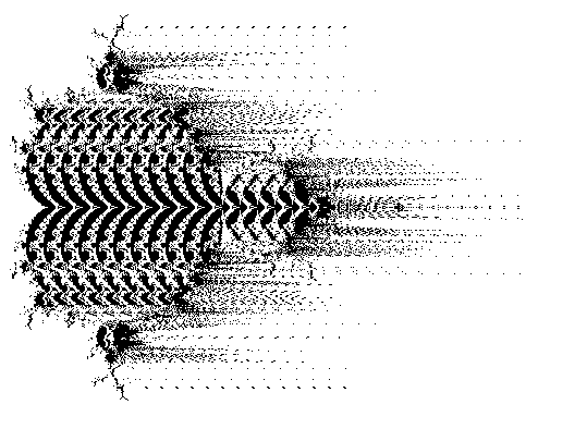
(This picture shows the result of a bug in my scheduler. Sometimes it is broken code that makes the coolest-looking results.)
With a working simulation, and a highly-visible counter that showed how many clock ticks were necessary to complete computation, I could work on optimization.
Optimization
Optimizing for this platform was a different experience than optimizing typical software. As well as taking less clock ticks to complete, the program also has to be optimized in space, to reduce the number of gates needed.
This led to behavior that I did not expect:
In typical software optimization, I will often check for conditions so that I can do less work if necessary, and skip going down an unneeded code path. In hardware, though, conditions are expensive, because each requires wiring.
"Skipping a code path" is sometimes meaningless - the entire path is done in one clock tick anyways, and it is taking up space, so it is often better to --always-- be performing the computation, and just ignore the result if it happened to not be needed.
Straightforward optimizations included tuning constants so that iterations decreased while the image quality is still acceptable. I set up initial conditions and coordinates to values that the Parent scheduler happened to work more efficiently with. I tightened up the state machine in the child module, coming up with a way to need only two states. I rewrote the scheduler so that it did not need a barrel-shifter. For the sum of two fixed-point products, I could right-shift the sum instead of the individual products. I moved most logic to assign= statements.
I could save significant time by skipping computation inside the inner 'cardioid' shape. I soon learned, though, that multiplication was expensive due the design I chose. There were limited hardware multipliers, and
I needed all children to perform at least 3 multiplies every clock tick. On the real hardware I had, there was no room for this shortcut.
Multiplication by a constant, though, I realized could be done very quickly. It was fun to re-write multiplication by 320, as n*320 == (n<<6) + (n<<8). Division by powers of 2, of course, I also converted into shifts.
I aggressively re-used computed values, such as how x2 and y2 could be used in both iteration and checking magnitude.
One attempt was to use an "approximation" abs(x)+abs(y) instead of the true magnitude, and to replace x2-y2 with (x+y)*(x-y), saving one multiply. This changed the
visual appearance in an odd way, though.
I was pleasantly surprised to see in the logs that the Xilinx software understood that the Child module was using a state machine, it apparently could place the state reg in a more efficient way.
Implementation
Developing with simulation can be misleading. You can use as much memory as you want, and it seems perfectly fine to multiply and even divide (!) numbers with just the symbols * and /.
On real hardware, RAM is limited, and in my case, hardware multipliers even more limited. One makes tradeoffs between longest chain of logic and clock speed.
Also, the software for synthesis has a learning curve, and synthesizing can take a significant amount of time.
I succeeded in synthesizing the project onto the hardware available to me, a Xilinx Spartan3 XC3s1500.
To make the image look interesting, I shifted the color palette over time, making the colors move.
The entire image is recomputed every time the colors shift, an intentional way of demonstrating how fast my system is.
As the video above shows, the results looked great, and the refresh rate was more than sufficient.
With the limitations of the specific hardware used, my final configuration was:
4 computing children
64 colors in palette
320x240 image
25Mhz clock speed
68,024 ticks to draw one frame at standard zoom
With a larger FPGA, I could have increased the number of children to drive these numbers higher. Even still, this math brought a smile to my face:
68,024 ticks to compute 76,800 pixels
68,024 ticks @ 25Mhz to compute 76,800 pixels
0.00272096 seconds to compute 76,800 pixels
1 second to compute 28,225,332 pixels
28 million computed values per second sounds pretty nice to me.